

Abstract
The strain relaxation, depth profiles of composition and density of dislocations in GeSn epilayers were studied by using the x-ray diffraction. Regions with uniform and graded composition, different levels of strain relaxation, and dislocation density were found in the GeSn layers grown at fixed growth conditions. At the initial stage of growth, the GeSn layer is under ∼8 × 10⁻³ compressive strain, and the Sn composition is close to the target value of 6.6%. With increasing layer thickness, the Sn content is enhanced by 0.85 ± 0.12% due to the relief of compressive strain down to ∼5.0 × 10⁻⁴. The plastic strain relaxation is dominated by 60° misfit dislocations at the GeSn/Ge interface, where their density is 3 × 105 cm−1. The relaxed GeSn layer serves as a buffer for the high-quality GeSn overlayer with uniform and enhanced Sn composition. The laboratory-based x-ray diffraction is shown as a non-destructive reliable technique for strain, composition, and defects characterization, as an alternative to secondary ion mass spectrometry and transmission electron microscope techniques.
Export citation and abstract BibTeX RIS
1. Introduction
Silicon (Si), germanium (Ge), tin (Sn) and their alloys are among the most promising materials for optoelectronics on the Si substrate platform [1, 2]. In fact, Si-based electronics already benefits from the excellent electronic properties of Ge [3]. In Si-based photonics, the quasi-direct bandgap of Ge is primarily used for passive photonic devices such as near-infrared detectors and optical modulators [4, 5]. However, more efficient absorption and emission processes can be achieved by making use of the direct bandgap of GeSn alloys [6]. Among the recently demonstrated GeSn photonic devices are near-infrared photodetectors [7], short-wave infrared light-emitting diodes [8], and low temperature optically and electrically pumped lasers [9, 10].
Fortunately, the conduction band energy of the indirect germanium L valley is only 140 meV below the direct Г valley [11, 12]. As a result, one approach to cause Ge to have a direct bandgap is to introduce tensile strain [13]. The limitations of this approach are serious, however, and include early plastic relaxation and very little potential for bandgap tunability [14]. Alternatively, the introduction of zero bandgap α-Sn into the crystal lattice of Ge is a more promising approach to reduce the energy difference between the L and Г points to cause an indirect-to-direct bandgap transition. The Sn concentration needed for this transition can be as low as 6% for unstrained [1] GeSn alloys and 9%–10% for compressively strained [15] GeSn alloys. An important advantage of this approach is the potential tunability of the direct bandgap by tuning the composition of the GeSn alloy. In this case, the bandgap can be tuned over a broad wavelength range that not only covers the typical communication wavelength window between 1.26–1.67 μm but extends to provide the opportunity for broad infrared lasers and detectors [16].
GeSn alloys can be achieved on Ge virtual substrates which grow under compressive strain due to the high lattice mismatch (∼15%) between Ge and α-Sn [9]. As a result of the larger atomic radius of tin (1.58 Å) than that of germanium (1.39 Å), Sn incorporation is restricted during the epitaxial growth [17] and coherent growth is maintained only at the initial stage of epitaxial deposition up to a critical layer thickness. Above the critical thickness, the compressive strain is plastically relieved by misfit dislocations (MDs) [18, 19]. Otherwise, upon the thermal treatment high densities of MDs may be observed below the critical thickness [20]. The mechanism of plastic relaxation was thoroughly investigated previously for the SiGe/Si heterosystem [21]. It was shown that for (001) oriented epilayers, the strain relaxation is governed mostly by 60° a/2 < 110 > {111} and 90° a/2 < 110 > {001} MDs, where a is the lattice parameter. The surface nucleated 60° MDs can easily glide along the {111} planes towards the layer/substrate interface and are commonly observed for low lattice mismatch (< 2%). Meanwhile, the sessile 90° MDs are the most effective plastic defects, and dominate the plastic relaxation only for large mismatch levels (> 2%) [22]. In either case, the relaxation of compressive strain in a GeSn layer can increase the Sn incorporation and can lead to the formation of an unintentional self-determined compositional gradient in the GeSn film at fixed growth conditions [23].
As a result, most studies on GeSn have a need to know how much Sn is incorporated into the lattice as well as the nature of the strain and defects. This can be accomplished by time-consuming and destructive secondary ion mass spectrometry (SIMS) or by transmission electron microscopy (TEM) techniques. In contrast, x-ray diffraction (XRD) is a well-established characterization technique that can simply and quickly be used for strain relaxation and structural quality investigation. In this paper, we demonstrate that comparison between measured and a calculated XRD reciprocal space map (RSM) provides an alternative to SIMS and TEM to obtain the (1) strain state, (2) composition, (3) density of MDs and (4) type of MDs [22, 24] for a compositionally graded layer.
Our results are reported on GeSn layers grown by chemical vapor deposition (CVD) on Ge/Si(100) substrates. The defect configuration of the epitaxial layers is retrieved by comparing the measured and calculated RSMs for an asymmetrical reflection. The calculations are based on the kinematic theory of diffuse x-ray scattering from epitaxial layers with misfit dislocations [24]. The strong lattice disorder due to MDs in thin films reduces the size of the coherent scattering regions, which justify the use of the kinematic theory. For GeSn/Ge/Si(100) heterostructures it is demonstrated that the strain relaxation is dominated by 60° MDs, and their density is considerably higher at the GeSn/Ge interface. The RSM simulations are used additionally to determine the depth profiles of Sn concentration in the GeSn layers and the interplay of the strain state and Sn incorporation. Finally, the depth distribution of Sn content was also confirmed by SIMS profiles to provide additional evidence for the value of our RSM simulations and comparison with x-ray data, as an alternative to SIMS and TEM.
2. Methods
Three samples containing GeSn layers were grown by CVD using an ASM Epsilon 2000 Plus reduced pressure system. A 700 nm thick Ge buffer layer was deposited on a Si(100) substrate prior to the GeSn growth. For all samples, the GeSn layer was grown at 300 °C with a SnCl4/GeH4 molar flow fraction of 8.5 × 10⁻³. The deposition time was 15, 50, and 75 min and the resulting GeSn layer thickness was 130, 750, and 1100 nm for sample S1, S2, and S3, respectively. For all samples, the target Sn composition was 6.6%. A 10 nm thick Ge cap layer was grown only on top of samples S2 and S3. The structural properties and the compositional profiles were uncovered with XRD. The XRD measurements were performed using Philips X'pert MRD system. The diffractometer was equipped with a standard four-bounce Ge(220) monochromator, 1.6 kW Cu Kα1 x-ray tube and a Pixel detector. The simulations of the XRD RSM were performed within the kinematic theory of x-ray diffraction.
3. Results and discussion
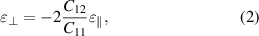
Figure 1 shows the geometry of a multilayer GeSn/Ge heterostructure and the ω/2θ scans measured across the Si(004) reflection for the three samples. The angular positions for the bulk Si and Ge are marked on the ω/2θ scans in figure 1(b) by the vertical dashed lines on the plot. The vertical lines near the GeSn peaks denote the fully strained (R = 0) and fully relaxed (R = 1) Ge93.4Sn6.6 alloy. For all samples, the peaks from the Ge buffer appear at the same angular position, but slightly right-shifted with respect to the position of bulk Ge. This indicates that the residual in-plane strain ( ) in the Ge buffer is tensile, and that the strain magnitude is not affected by the GeSn layer thickness. The value of
  can be estimated from the peak position of Ge using the Bragg's law in the form,

and the biaxial strain relation
where  and
and  are the in- and out-of-plane strain components,
  and
and  are the actual in- and out-of-plane lattice parameters,
  = 0.5658 nm is the lattice parameter of unstrained Ge, and
  = 126.5 GPa and
  = 48.3 GPa are the elastic constants of Ge [25].
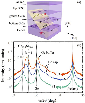
Figure 1. (a) Schematic illustration of a multilayer GeSn/Ge heterostructure with networks of 60° misfit dislocations (MDs) at the interfaces and the motion of a threading dislocation (TD) from the Ge buffer layer. (b) X-ray diffraction ω/2θ scans measured across the symmetrical Si(004) reflection for samples S1, S2, and S3. The dashed vertical lines indicate the positions for the bulk Si and Ge, as well as of fully relaxed (R = 1) and fully strained (R = 0) GeSn-on-Ge.
Download figure:
Standard image High-resolution imageFor all samples, the Ge buffer is under 0.19% tensile strain. This value is in good agreement with reported 0.2% for Ge-on-Si(100) [25, 26], where the tensile strain was attributed to the thermal expansion coefficient mismatch between Ge and Si. For samples S2 and S3, the weak Ge peaks at ω = 33.2 deg are associated with the Ge cap, which points to a much larger tensile strain as compared to the Ge buffer. In fact, the thin Ge cap adopts the in-plane lattice parameter of the underneath GeSn layer that must be strain relaxed. This is confirmed below on the RSM (see figure 2), where the peak from the Ge cap is vertically aligned with that of underneath GeSn layer. A similar peak is not observed for sample S1, which is grown without the cap layer. The actual Sn content and strain state of the GeSn layers cannot be confirmed from the peak position on the ω/2θ scan since strain relaxation or a decrease of Sn content would result in a similar GeSn peak shift toward the higher angular values. This can be seen by comparing the positions of the vertical lines for the fully strained (R = 0) and fully relaxed (R = 1) Ge93.4Sn6.6 alloy. Moreover, given the thickness-dependent strain relaxation and the different thickness of the GeSn layer for samples S1 (130 nm), S2 (750 nm), and S3 (1100 nm), the strain state is expected to be different for each sample.
Figure 2. Measured RSMs around the asymmetrical Ge( ) reflection for sample S1 (a), S2 (b), and S3 (c). The vertical and inclined dashed lines mark the positions of the fully strained (R = 0) and fully relaxed (R = 1) Ge1-xSnx alloy, respectively.
Download figure:
Standard image High-resolution imageHowever, the strain and composition in the GeSn layers were determined by measuring the RSM around the asymmetrical Ge( ) reflection. Figure 2 depicts the RSMs containing the peaks from the Ge buffer and GeSn layers. The GeSn peaks fall in between the fully strained (R = 0) and fully relaxed (R = 1) lines, which indicates strain relaxation. For sample S1, the slight shift of the GeSn peak towards the relaxation line indicates that the critical thickness for strain relaxation is just under 130 nm, which is the thickness of the GeSn layer for this sample. The shift increases with the layer thickness and is accompanied by a strong diffuse scattering that surrounds the peak due to an increase of MDs density [24]. For samples S2 and S3, the GeSn peak shows regions with the different Sn composition that are marked by arrows on the RSM. At fixed growth conditions, we observe in figure 2 that an enhanced Sn incorporation occurs together with the progressive relaxation of the compressive strain in the GeSn layer consistent with other reports [23]. Accordingly, for S2 and S3 the Sn content in the uppermost part of the layer is higher than in the bottom part. On the RSM this corresponds to the peak at the lowest
  . The Sn concentration (
 ) was resolved from the peak position on the RSM, which provides the actual lattice parameters
  and
and  by
by
The substitution of  and
and  in equation (2) allows estimating the relaxed lattice parameter (
 ) of the GeSn alloy as follows
where the elastic constants  and
and  and the lattice parameter
  of the GeSn alloy are given by linear interpolation between the parameters of Sn and Ge, such as
  [27].
[27].
The Sn content was determined from the most intensive GeSn peak on the RSMs, and  was 6.70, 7.86, and 7.25% for samples S1, S2, and S3, respectively. Note, for S2 and S3 this is the concentration in the upper part of the GeSn layer. The concentration in the bottom part cannot be precisely resolved due to the uncertainty of the peak position determination. As a result, the strain state in the bottom part of the GeSn layer remains unknown, which obstructs studying the role of strain relaxation on the process of Sn incorporation. The close vicinity of the GeSn peaks on the RSM additionally alters the peak shape, which otherwise provides the type of MDs [24, 28].
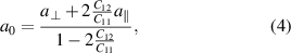
Overcoming these limitations, the profiles of composition, strain, and dislocation density in the GeSn layers are extracted from comparison between the RSM experiment data and simulation. The theoretical description of x-ray diffuse scattering by a layer containing MDs was developed by Kaganer et al [24]. The necessary expressions of the theory are shortly summarized below. For an epitaxial film with a large density of uncorrelated MDs, the scattered intensity is given by the following equation
where  is the GeSn layer thickness,
  are the components of the reduced scattering vector
  ,
,  stand for
  ,
,  is a
is a  symmetrical matrix with the elements
  , and
, and  are the elements of the reciprocal matrix
  . Equation (5) takes into account the fact that the beam is not collimated normal to the diffraction plane, which gives rise to a delta function when integrating over the
  component of the scattering vector [22, 29].
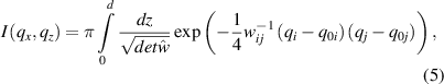
The quantities  and
and  in equation (5) are proportional to the density of MDs, and in the reciprocal space determine the shift and broadening, respectively, of the diffraction peaks. In the absence of crystallographic tilt between an epitaxial film and the substrate, the expressions for
  and
and  for a multilayered structure are given as [22]
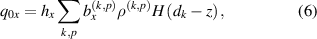
where  is the linear density of MDs of type
  at the
  th interface;
  is the Poisson ratio;
  is the strain relieving component of the Burger's vector, which is
  and
and  for 60° and 90° MDs, respectively;
  is the step-like Heaviside function;
  is the composition related shift of the diffraction peak on the RSM
where  is the lattice mismatch between the layer and substrate. The absence of crystallographic tilt between the GeSn layer and Ge substrate was confirmed for all samples by measuring the ω scans around the 004 reflection at different azimuths (not shown here).
It should be noted, the quantities  and
and  in equations (6)–(8) are proportional to the Burgers vector and its square, respectively. Accordingly, the strain field of 60° MDs with
  and 90° MDs with
  produce a different shift and orientation of the diffuse scattering on the RSM, and this is the basis for the precise determination of the type and density of MDs. As a result, we can unambiguously identify the density and type of misfit dislocations. The early work of Kaganer et al [24] clearly demonstrated the effect of different types of misfit dislocation on the x-ray diffraction diffuse scattering. The strain fields of different types of misfit dislocations sufficiently differ, and x-ray diffraction is sufficiently sensitive to small changes in the lattice parameter, which together support our report of density, type, and distribution of misfit dislocations.
For the simulation, the GeSn layer was divided into three sublayers to be in agreement with our experimental results from the three samples and consistent with previously demonstrated structure of relaxed GeSn films [23]. The concentration of Sn is uniform in the top and bottom sublayers and graded in the middle sublayer. The compositional gradient in the middle layer is linear and is defined by the lowest and highest Sn content in the bottom and top sublayers, respectively. Both 60° and 90° MDs were allowed at the GeSn/Ge interface and at the interfaces between the sublayers. However, the fitting results indicate that the strain relaxation is dominated by the 60° MDs. The measured and calculated  RSMs are compared in figure 3 for samples S2 and S3. A good fit of the measured RSMs is seen in the inset of figure 3, which compares the scans extracted from the experimental and calculated maps.

Figure 3. Measured and simulated RSMs around the asymmetrical GeSn( ) reflection for samples S2 (a, b) and S3 (c, d). The inset compares the extracted cuts over the measured (black line) and simulated (red line) RSMs.
Download figure:
Standard image High-resolution imageFigure 4 compares the depth profiles of Sn content in the GeSn layers of the three samples. Here we also compare the approach using our RSM data and simulations in this research to an approach using SIMS. The dotted lines depict the SIMS measurements and the solid lines show the Sn profiles obtained from the RSMs data and simulations. For sample S1, the composition is uniform throughout the GeSn layer and the content of Sn is 6.70%. Three regions with different Sn content can be observed for samples S2 and S3. The regions of uniform composition are seen at the bottom and top parts of the GeSn. The Sn content in the shortest bottom part is close to the target value and is 6.90 and 6.55% for samples S2, and S3, respectively. The middle layer has a graded composition with a gradient of 4.4 ± 0.1 %/µm. For both samples, the bottom and graded regions extend over the 65 ± 15 nm and 185 ± 15 nm, respectively. The top part of the layer is the most prolonged, and the Sn content is enhanced to 7.86 and 7.28% for samples S2 and S3, respectively.

Figure 4. The depth profiles of Sn in the GeSn layers of sample S1, S2, and S3 obtained from SIMS measurements (dotted line) and RSM simulations (solid lines).
Download figure:
Standard image High-resolution imageIt is important to note that our model does not consider the possibility of Sn precipitations [30]. There are three reason for this approach: (1) no Sn precipitation was observed in the x-ray spectrum for our samples, even for S1 with no cap, for which the GeSn is fully strained to the Ge substrate; (2) if Sn precipitation existed and played a role in our reported profile, it would have impacted the profile in S1 for which RSM gives a constant Sn profile, which is also supported by the SIMS profile. While (1) and (2) indicate no evidence for Sn precipitation, even though the RSM and SIMS studies do not investigate Sn precipitations, (3) the excellent agreement between RSM and SIMS, means that it is not necessary to assume Sn precipitations to explain either our x-ray data or the confirming SIMS data.
The likely explanation for the uniform and compositional grading is the observed different strain state in the three regions of the GeSn layer. For the given Sn content, the GeSn layer of sample S1 is under 8.2 × 10⁻³ compressive strain when it is fully strained to the Ge buffer. As a rough approximation, the critical thickness for strain relaxation, in this case, is between 50 and 100 nm [31], which is much like the thickness of the GeSn layer of sample S1 (figure 4). According to the XRD measurements, the residual compressive strain in the GeSn layer of sample S1 is uniform and its value is 7.4 × 10⁻³ (figure 5). Therefore, the uniform composition can be related to the uniform compressive strain in the nearly fully strained GeSn layer. This is also justified for the bottom part of the GeSn layer of samples S2 and S3. The Sn content, in this case, is uniform until the critical thickness is reached (< 100 nm). Above the critical thickness, the strain is relieved by 60° MDs. The gliding of MDs towards the GeSn/Ge interface gradually reduces the lattice mismatch as well as the magnitude of the compressive strain. This triggers a gradual enhancement of the Sn incorporation in the layer which grows upon the critical thickness. When the residual compressive strain at the bottom GeSn layer is reduced to ∼5.5 × 10⁻⁴, the new MDs do not form. Without the nucleation of new MDs, the incorporation of Sn in the growing top region of the GeSn layer is under the condition of uniform strain. Accordingly, the uniform Sn content in this part of the layer can be also associated with the uniform compressive strain.

Figure 5. The compressive strain and the density of MDs in the GeSn layer near the Ge/GeSn interface. The inset shows the compressive strain as a function of the lattice parameter in the bottom and top regions of the GeSn layer of sample S2 and S3. The scatters represent the experimental data, and the lines depict the calculated lattice parameter for varying compressive strain at constant Sn content.
Download figure:
Standard image High-resolution image
For sample S2 and S3, the density of 60° MDs at the GeSn/Ge interface is much higher than for sample S1 and is about 3 × 105 cm−1 (right axis of figure 5). Nearly the same MDs density for the two samples is related with the same lattice mismatch between the GeSn layer and Ge buffer. Moreover, the same grading rate ∼4.4 ± 0.1%/µ of the Sn content for the both samples serves as an additional indication that the strain relaxation is relieved by the same type of MDs. Otherwise, the nucleation of edge type MDs, which are more effective in relieving strain, would result in a more rapid relaxation and thus higher compositional gradient. The observations for the three samples indicate that the critical thickness for strain relaxation is near 100 nm, and the gradual Sn enhancement is facilitated by the compressive strain relaxation and nucleation of 60° MDs.
Our simulations did not include threading dislocations. The reason is that, given the high density of misfit dislocations in our samples (105 cm−1) the influence of the threading dislocations (108 cm−2) on x-ray scattering data is negligible and we can neglect them. The negligible small role of TDs on the x-ray diffuse scattering was found and explained previously for PbTe/Si heterosystem [32]. It should be noted, that the density of misfit dislocations compared to the density of threading dislocations was of the order of 104 cm−1 to 108 cm−2, respectively, which is comparable with our GeSn/Ge samples. Moreover, the MDs are not limited by the film thickness and extend at longer distances than TDs. Therefore, it can be concluded that the misfit dislocations are very much stronger defects than threading dislocations for strain relaxation in GeSn/Ge heterosystem.
The role of compressive strain relaxation on the enhanced Sn incorporation can be further understood by analyzing the  as a function of the lattice parameter
  (inset in figure 5). The scatters on the plot stand for the actual
  and
and  in the bottom and top parts of the GeSn layer. For samples S2 and S3, the level of compressive strain is about the same in the bottom part of the GeSn layer and slightly larger in the top region due to the enhanced Sn content. The solid and dashed lines in the inset trace the change of the lattice parameter with varying compressive strain at constant composition. An important observation is the increasing lattice parameter with the Sn content at
  . The larger lattice parameter must be more favorable for the incorporation of Sn atoms into the crystal lattice of Ge. Accordingly, for a fully relaxed GeSn layer, the spontaneous gradient and the Sn content enhancement must be higher for a layer with a higher initial Sn composition.
While we have explained that the changes in the Sn concentration are due to changes in the stress level an alternative explanation is that segregation of Sn occurs in the GeSn film growth [33, 34]. However, there are two reasons to not assume segregation in our samples: (1) No physical evidence of segregation was observed for sample S1, for which there is no cap and for which the GeSn is fully strained to the Ge substrate; (2) For sample S1, x-ray data shows a constant Sn composition. Accordingly, if we were to assume that segregation is taking place, it does not lead to an observed compositional gradient in the x-ray. Therefore, for our samples, segregation cannot be the driver of the observed composition gradient.
4. Conclusions
In this work, the relationship between the compressive strain relaxation and the enhanced Sn incorporation in the GeSn/Ge/Si(100) heterostructures was investigated using XRD techniques. We demonstrated that comparison between measured and a calculated XRD reciprocal space map (RSM) provides an alternative to SIMS and TEM to obtain information on sample strain, composition, and density and type of MDs.
For fixed growth conditions, a GeSn layer was characterized with regions of uniform and graded Sn composition spontaneously formed at the different growth stages. In a fully strained layer, the Sn content is close to the target value of 6.6%. The enhanced Sn incorporation was observed with the onset of 60° MDs nucleation, which formed in order to reduce the 0.8% lattice mismatch at the GeSn/Ge interface. For the given mismatch, the compressive strain in the GeSn layer was reduced from ∼8.2 × 10⁻³ to ∼5.5 × 10⁻⁴ during the growth of a 185 ± 15 nm thick GeSn layer. This region has a graded Sn content with a grading rate of 4.4 ± 0.1 %/µm for each sample. Above it, the growth resulted in a high-quality GeSn layer with an enhanced uniform Sn content of 7.5 ± 0.3%. As a result, x-ray diffraction is demonstrated as a non-destructive and reliable technique for strain, composition, and defects characterization.
Acknowledgments
This work was supported by Multidisciplinary University Research Initiatives (MURI) Program through the U.S. Air Force Office of Scientific Research (AFOSR) Grant No. #FA9550-19-1-0341.